Individual Wafer Control
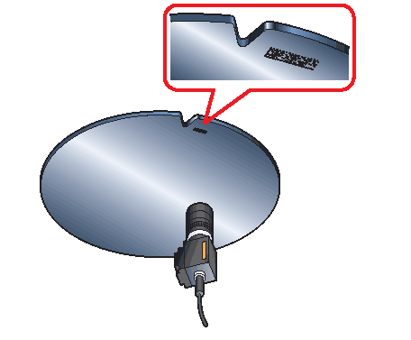
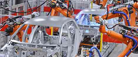
Problem: Until now, in the production of DRAM, for example, wafers have usually been processed in lots of 25 (i.e., in wafer carrier units). The switch, however, towards high-diversity, low-volume production (e.g., custom LSI) has made individual wafer control necessary. In order to avoid reducing the number of IC chips produced per wafer, the markings used for individual wafer control must be as small as possible. Mark the back surface of each wafer with wafer ID (2-dimensional code) satisfying the specifications of the SEMI T7 standards using a laser marker. (The surface can be marked with a wafer ID consisting of 13 alphanumeric characters in an area of 4 × 1 mm.) When the wafers are introduced into the processing equipment, read the wafer ID (2-dimensional code) with a 2-Dimensional Code Reader and send the information to the equipment.
 Automation Systems
  Motion & Power Solutions
  Safety, Vision and IDENT
  Sensing Solutions
  Control Components
  Switching & Accessories
  Switchgear and Trolley Systems
  Process Weighing
  LED Lighting
  Omron
Omron
 Mitsubishi
 Delta
Delta
 Autonics
 Inno
Inno
 Panasonic
 Novotechnik
 Orientalmotor
 Microscan
 IPA
IPA
 Technomech
 Intech
 Honeywell
 IOT & Traceability
 Project & Panel Engg.
 Application Case Studies
 Solutions by Industry
 Solutions by Process
 Solutions by Product
 Youtube Videos
 Corporate Information
 Company Profile
 Quality Policy
 Mission Statement
 Chairman's Message
 Intech Group Companies
